Welding inverter is an alternative to a conventional welding transformer. Modern semiconductors allow to replace the traditional mains transformer with a
switching power supply, which is much lighter, smaller and allows easy current adjustment via a potentiometer. The advantege is
also that the output current is DC. DC current is less dangerous than AC and prevents arc extinction.
For this inverter i chose topology, which is the most common in welding inverters - forward converter with two switches.
In my article about switchning supplies it is a topology II.D.
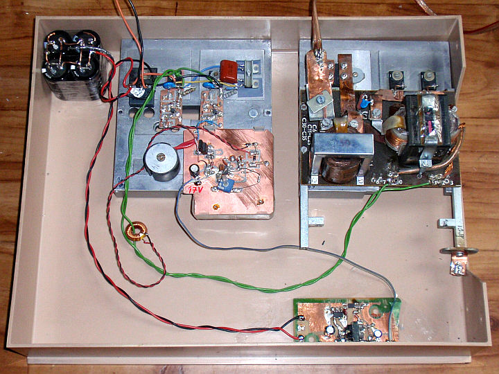
Input mains voltage passes through an EMI filter and is smoothed with high capacity capacitors. Since the inrush current of those capacitors would be too high,
there's a softstart circuit. After switching ON, the primary smoothing capacitors are charging via resistors, which are later bypassed
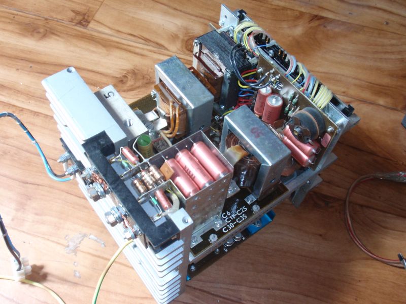
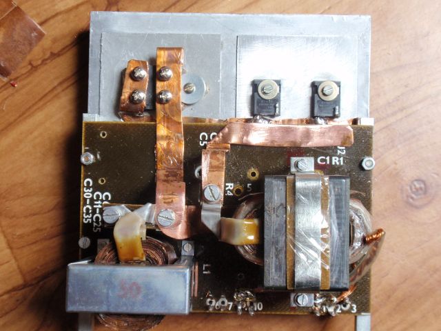
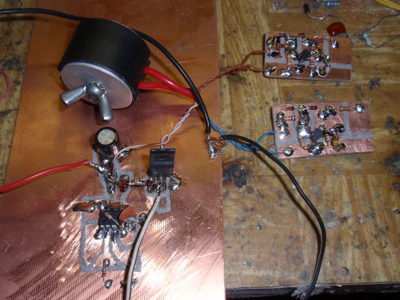
by the contact of a relay. As power switches, IGBT transistors IRG4PC40W are used.
They are driven through a forward gate-drive transformer TR2 and shaping circuits with BC327 PNP transistors.
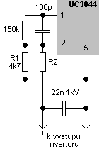
The control integrated circuit is UC3844. It's similar to UC3842, but it has its pulse-width limited to 50%. Working frequency is 42kHz.
Control circuit is powered by an auxiliary power supply of 17V.
Current feedback, due to high currents, is using a current transformer Tr3. Voltage drop accros the sensing resistor 4R7/2W is approximately proportional to the output current.
Output current can be controlled by potentiometer P1, which determines the threshold of the current feedback. Threshold voltage of the pin 3 of UC3844 (current sensing) is 1V.
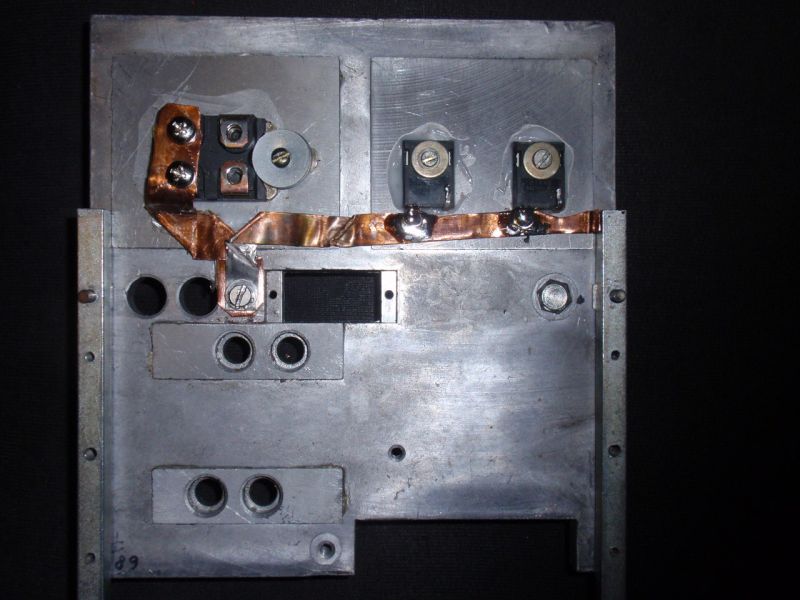
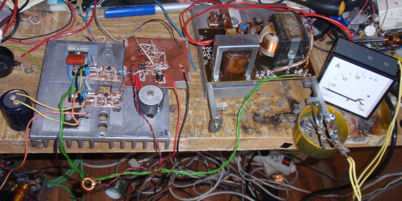
Power semiconductors require cooling. Most of the heat is dissipated in output diodes. Upper diode, consisting of 2x DSEI60-06A, must in worst
case handle the average current of 50A and the dissipation of 80W (total of both diodes).
Lower diode STTH200L06TV1 (doube diode package with both internal diodes connected in parallel) must in worst
case handle an average current of 100A and the dissipation of nearly 120W. Maximum total dissipation of the secondary rectifier is 140W. The heatsink must be able to handle it.
To the thermal resistance you must include the junction-case Rth, case-sink Rth and sink-ambient Rth.
DSEI60-06A diodes don't have insulation pads and the cathode is connected to the the heatsink. Output choke L1 is therefore in the negative rail. It
is advantageous because in this configuration, there's no high-frequency voltage on the heatsink.
You can use another type of diodes, for example a parallel combination of a sufficient number of the most accessible diodes,
such as MUR1560 or FES16JT. Note that the maximum average current of the lower diode is twice the current of the upper diode.
Calculation of the power dissipation of the
IGBTs is more complicated because in addition to conductive losses there are also switching losses. Loss of each transistor is up to about 50W.
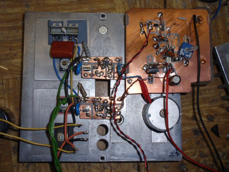
It is also necessary to cool the reset diodes UG5JT and the mains bridge rectifier. The power dissipation of the reset diodes depends on the construction of Tr1
(inductance, stray inductance), but is much lower than the dissipation of the IGBTs. The rectifier bridge has a power dissipation of up to about 30W.
UG5JT diodes and the rectifying bridge are placed on the same heatsink as the IGBTs. UG5JT diodes
also can be replaced with MUR1560 or FES16JT or other ultrafast diodes.
During construction it is also necessary to decide the maximum loading factor of the welding inverter, and accordingly select size of heatsinks, winding gauges and so on.
It is also good to add a fan.
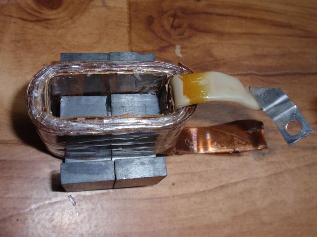
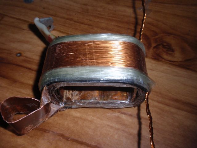
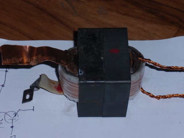
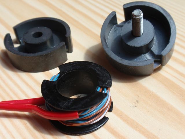
Switching transformer Tr1 is wound on two ferrite EE cores, each with a central column cross section 16x20mm. The total cross section is therefore
16x40mm, the core must have no air gap. 20 turns primary winding is wound using 14 wires of a 0.5 mm diamater. It would be better to use 20 wires, but they
didn't fit into my core.
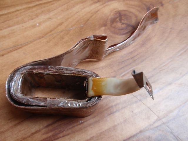
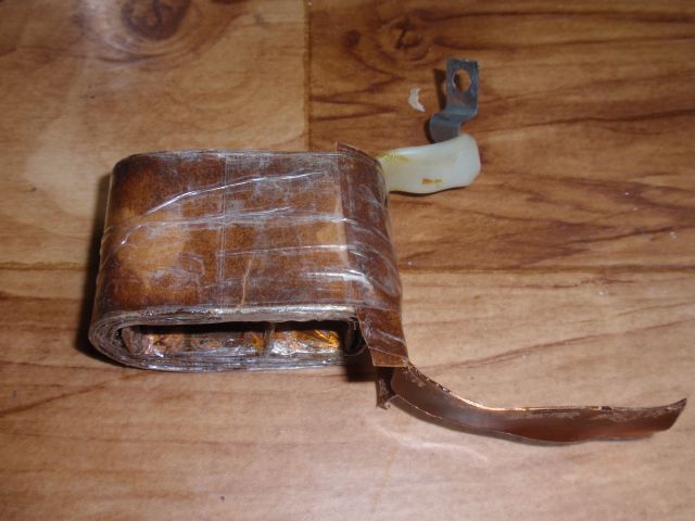
Secondary winding has 6 turns of a copper strip (36 x 0.5 mm). Forward gate-drive transformer Tr2 is made with an emphasis on low stray inductance. It is trifillary wound,
using three twisted insulated wires of 0.3 mm diameter, and all the windings have 14 turns. Core is made of material H22, middle column has a diameter of 16mm, with no gaps.
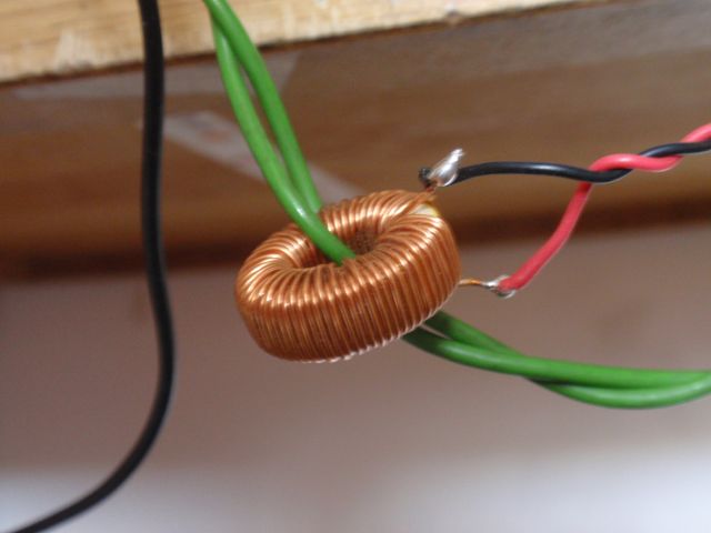
Current sensing transformer Tr3 is made from an EMI suppression choke on a toroidal core. The original winding with 75 turns of 0.4 mm wire works as a secondary.
Primary has just 1 turn. Polarity of all the transformer windings must be kept (see dots in schematic)!
L1 inductor has a ferrite EE core, middle column has cross section 16x20mm. It has 11 turns of a copper strip (36 x 0.5mm) and the total air gap in the magnetic circuit is 10mm.
Its inductance is cca 12uH.
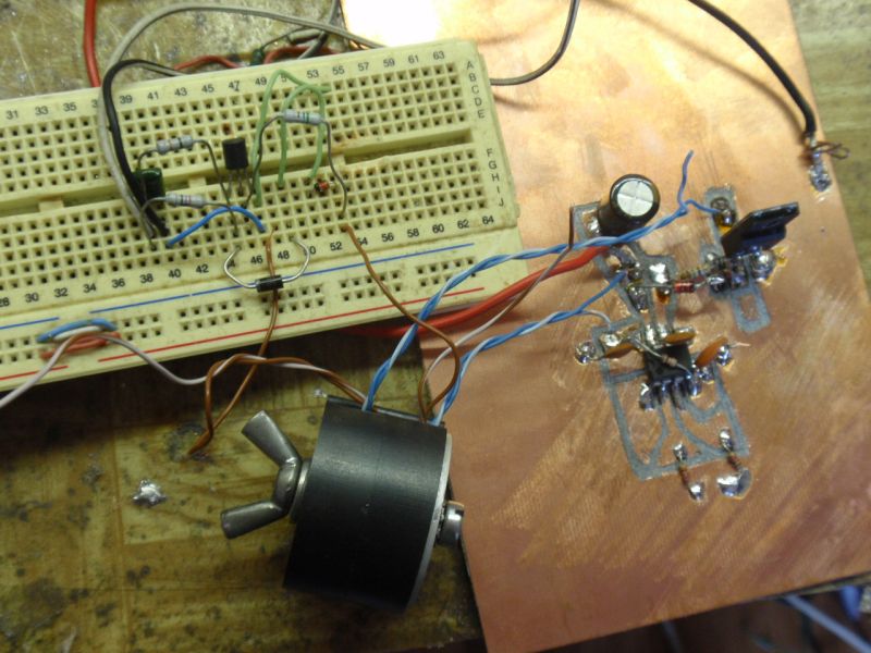
The auxiliary 17V switching power supply, including Tr4, is described in more detail
here.
The simplest welding inverter on Pic 1 has no voltage feedback. Voltage feedback does not affect the welding, but affects the power consumption and heat losses in the idle state.
Without the output voltage feedback there is quite high output voltage (approximately 100V)
and the PWM controller ia running at its max duty cycle, thereby increasing the power consumption and heating of components.
Therefore, it is better to implement the voltage feedback. You can inspire on Pic 2. The feedback can be connected directly because the controll circuit is
isolated from mains. The reference voltage is 2.5V. Select the R2 to set the open circuit voltage.
You can find useful info in datasheet of UC3842, 3843, 3844, 3845 or in its another datasheet.
Inspiration for modifications you can also find in 3-60V 40A supply.
Interesting links from which I drew:
http://svarbazar.cz/phprs/index.php?akce=souvis&tagid=3
http://leo.wsinf.edu.pl/~leszek/spawarki/
http://www.y-u-r.narod.ru/Svark/svark.htm
http://www.emil.matei.ro/weldinv3.php
http://nexor.electrik.org/svarka/barmaley/kosoy/shema.gif
and a little modified: http://nexor.electrik.org/svarka/barmaley/kosoy1/shema.gif
During your search, you may encounter websites offering a or similar cracked activation codes. While the promise of free, premium software is tempting, using patched license keys and cracked software downloads poses severe security risks to your computer and mobile devices. What is PassFab Android Unlocker?
Compatibility patches for the latest Android operating system updates and security patches.
Follow On-Screen Instructions: The software will guide you through putting your phone into Recovery Mode or Download Mode to perform the bypass. Official Alternatives and Free Methods
Searching for "passfab android unlocker 22016 key patched" is an unreliable and dangerous method for solving a device lockout. The threat of malware, data theft, and broken software far outweighs the cost of a legitimate license or the time spent utilizing free built-in Android recovery tools. For a secure resolution, stick to official Google recovery options, manufacturer tools, or authorized software channels. passfab android unlocker 22016 key patched
If you're looking to unlock an Android device and are considering using PassFab Android Unlocker or similar tools, here are some general points to consider:
Do you know the details linked to the device?
Websites promoting terms like "22016 key patched" or "keygen" rarely provide clean, functional software. Downloading modified executable files or applying unauthorized patches exposes your digital life to significant threats. 1. Malware and Trojan Infections During your search, you may encounter websites offering
The patched version of PassFab Android Unlocker 2.2.16 offers the following features:
PassFab Android Unlocker is a desktop utility developed to assist users who have been locked out of their smartphones or tablets. Legitimate use cases include forgetting a password, buying a secondhand device with an active lock, or troubleshooting a phone with a broken screen that prevents input. The software primarily focuses on two main features:
This is the most immediate and severe risk. When you download cracked software from unofficial websites, you are trusting anonymous uploaders who have no accountability. These files are frequently modified to include hidden payloads: The threat of malware, data theft, and broken
You do not need to risk downloading dangerous cracks to unlock your phone. Try these built-in, secure methods first. Method 1: Use Samsung’s "SmartThings Find"
Crack distribution sites often serve as delivery systems for malicious payloads. When you download a patched activation key or crack installer, you often secretly download keyloggers, infostealers, or ransomware. Because lock-removal tools require deep administrative privileges to communicate with connected USB hardware, a malicious patch gains deep access to your computer's operating system. 2. Device Brick Vulnerabilities
PassFab Android Unlocker is a legitimate desktop program.It is designed to help users regain access to their mobile devices.The official software offers several core features:
Note: This will wipe the phone, but it allows you to set it up as new. Samsung "SmartThings Find"
Software that records every keystroke to steal credentials. Ransomware: Encrypting user data for financial extortion. 2. System Instability